New generation of cyber-physical systems
PPS3 is focused on creating a new generation of cyber-physical systems. This raises several challenges, which are currently being addressed by the project, namely:
- Perception: related to the sensors needed to monitor the surrounding environment. These sensors must have low power consumption, be compact (small size) and low cost.
- Autonomy: related to the energy consumption of the complete system and the fault tolerance during operation. The important aspect of this challenge is to ensure long-lasting operation with a battery (for remote applications) and to ensure that the system does not need physical maintenance (use of over-the-air firmware updates).
- Security: related to data privacy (message encryption and information source validation)
- Availability: related to two-way communication at any location.
- Adaptability: related to the upgradeability and flexibility to address different use cases with the same hardware platform (through firmware upgrade)
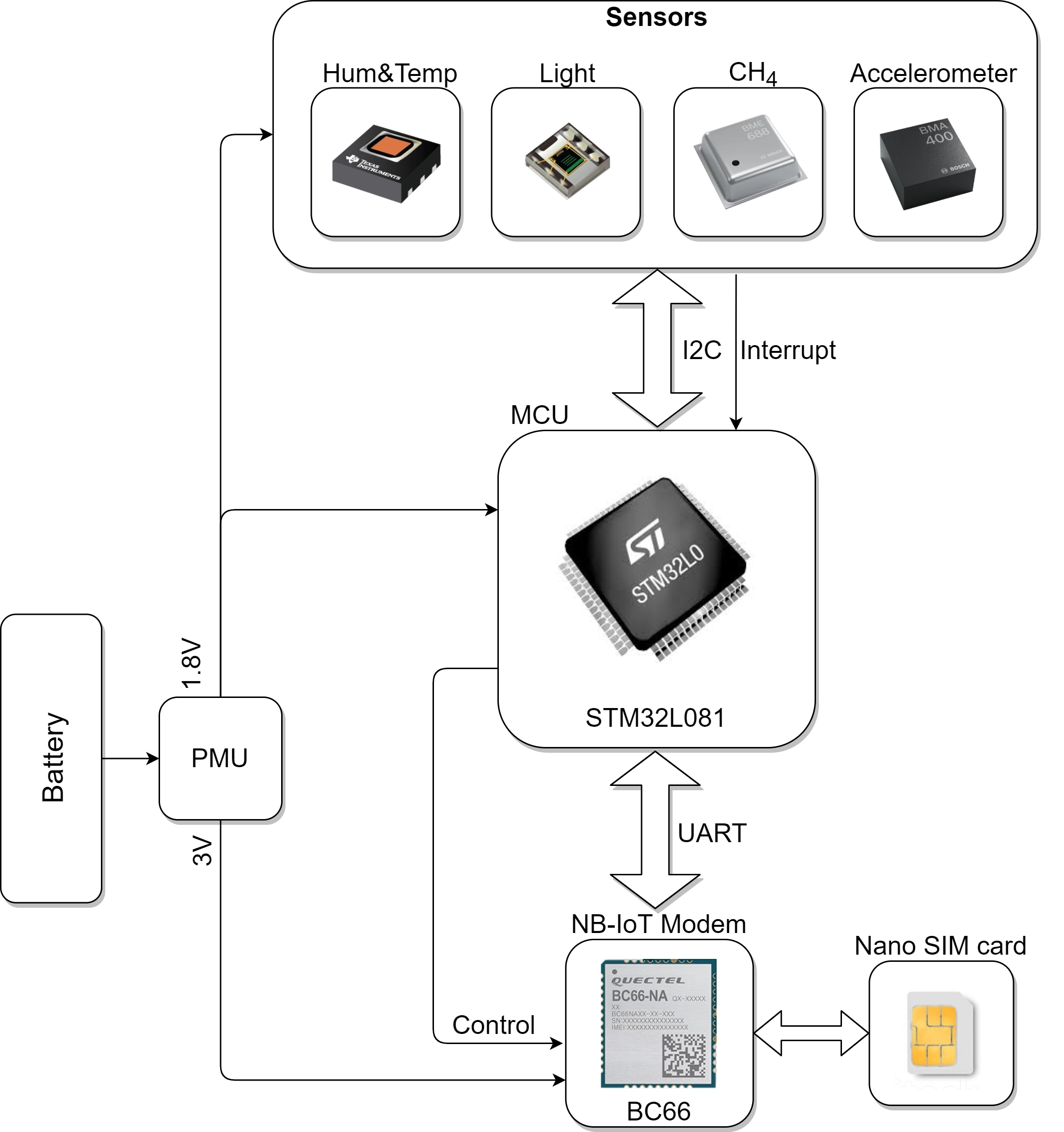
The basic architecture of the device can be seen in figure 1. The device is composed of: (i) sensors, for environmental monitoring (temperature, humidity, gas, vibrations/accelerations); (ii) a microcontroller, to handle data processing, encryption and storage; (iii) a battery, to power the device, and different modes of operation to reduce power consumption; and (iv) a communication modem, to handle the data transfer.

Figure 1 – CPS base architecture
The project already has four hardware iterations (see figure 2). From left to right in the figure, the first iteration focused on validating the system and its technologies. The second iteration was aimed at improving the size and manufacturing cost of the solution. The third version was adapted to fit the encapsulation that would be used in scenarios with real-world conditions. The fourth version allowed testing of the design of an antenna embedded in the PCB itself, which could improve communications. Currently the project is in its fifth iteration, where modularity and immunity to magnetic interference is being implemented.

Figure 2 – CPS iterations
Along with hardware versions, the firmware of the device is also continuously updated. It started with a bare-metal application that allowed sensor data to be read and sent immediately to the cloud, and evolved into a version with FreeRTOS in an attempt to improve the modularity of the application. However, the gains were not remarkable and it was decided to develop a new bare-metal version that allowed to save the data read by the sensors and only send them after a certain period of time, thus reducing the number of transmissions per day and, consequently, the total energy consumption. After this iteration, encryption was added to the data being transmitted in order to protect communications, as the possibility of remote configuration of the device via commands sent by the server was also added. In the last of the most significant iterations, ThreadX was added, allowing the idea of the second iteration to be taken up again, but with much more noticeable gains, allowing power consumption to be reduced and the modularity of the system to be increased, as well as its performance. In the latest version it was also added the possibility of updating the firmware over-the-air, that is, updating the firmware remotely, without the need for physical contact with the device.
The developed devices are currently in a testing phase in scenarios with conditions close to the real ones, to validate and improve them. Meanwhile, another line of work seeks to migrate this same system to FPGA platforms and ASIC technology, which allow large-scale fabrication of a custom chip for LINK4S. At the current stage of the work there are two processor architectures to be implemented in the custom microcontroller: Arm Cortex-M1 (optimized for FPGA, it would be replaced by the equivalent Arm Cortex-M0+ if used for ASIC manufacturing) and RISC-V (an open-source architecture that allows customization of the processor itself if needed).
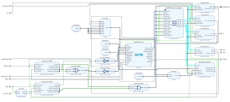
The FPGA system with the Cortex-M1 is already developed and validated with the remaining hardware, successfully replicating the functionality of the devices already in tests. This system has only the necessary peripherals for the foreseen functionalities and a sleep controller that allows replicating some modes of operation with lower power consumption (see image 3 for a better understanding of the blocks that make up the system in FPGA with Cortex-M1). In parallel, the solution is being developed using a RISC-V based microprocessor, which requires some more implementation effort regarding the necessary peripherals, but will allow an easier transition to ASIC manufacturing (see image 4 for a better understanding of the blocks that compose the system in FPGA with RISC-V in its current state).

Figure 3 – Cortex-M1 FPGA block diagram

Figure 4 – RISC-V FPGA block diagram
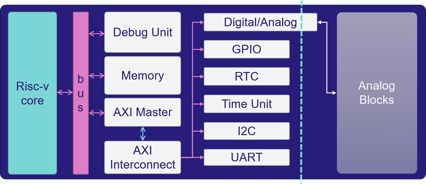
Once FPGA testing with RISC-V based architecture is complete, the system can be migrated to ASIC technology. The planned architecture for the microcontroller under development, including the digital and analog components, is shown in figure 5.

Figure 5 – RISC-V based architecture for the customized microcontroller
